Apr 17, 2011

Pulse-Width Modulation

Ok, I know it has been a while since I have posted anything but I doubt my two readers are losing any sleep over it. This post will finally discuss the long-awaited topic of pulse-width modulation (PWM).

PWM is a highly efficient control scheme used to manipulate the flow of power through various electronic devices. I have seen it most commonly used in switched-mode power supplies, LED dimming circuits, and variable speed motor controls, but there are several more applications. The concept of PWM draws from the most basic elements of a binary system: on (1) or off (0). At any given moment, switches are turned on or off depending on the feedback signal from the load receiving power. This process allows power to be taken from the source in doses and supplied to the output such that the output remains relatively constant. Exactly how much power is supplied to the load depends on the duty cycle of the switching system.

The duty cycle of a PWM waveform refers to the amount of time relative to an entire switching period that the pulse stays high. It is usually expressed as a percentage or decimal and can vary anywhere between 0% (completely off) to 100% (completely on). Figures 1-3 show some examples of various duty cycles used for voltage regulation and the math explaining how the load sees an average voltage depending on the switching conditions. The figures assume the switches are operating at 50 kHz (being turned on and off 50,000 times/second). 

Figure 1. PWM pulse train at a 20% duty cycle


Figure 2. PWM pulse train at a 50% duty cycle
 

Figure 3. PWM pulse train at a 80% duty cycle


In practice, PWM can be implemented in power supplies if the source power is switched at a sufficiently high frequency such that the output inductor can supply current without letting it fall to zero. Current passing through an inductor cannot change instantaneously which means even if the switch from the source is turned off the inductor current will drop steadily instead of falling to zero immediately. As long as the switch comes back on before the inductor current falls too low to be useful, the load sees a continuous flow of current.

Similarly, LEDs can be dimmed using PWM. By turning the LEDs on and off at a higher frequency than the human eye can detect, and varying the duty cycle, you can control the brightness level. A pulse train with a higher duty cycle will increase the brightness and vice versa. There is still some debate among the experts in the field of LEDs on what the minimum switching frequency should be but in general it can be as low as a few hundred hertz.

Lastly, PWM schemes are utilized with motors to regulate the speed of rotation. As long as the switch is turned on before the motor has a chance to decrease appreciably in speed, the motor will continue to perform its intended function.

So why is this scheme better than, say, adding a resistor to drop the voltage before it gets to the external load? The answer is efficiency. In any power transfer system, resistive elements are the enemy because they constantly create voltage drops and power loss. The beauty of including switching elements into a power transfer circuit is that the instantaneous losses are significantly reduced. When the switch (transistor) is open, no current is passing through the device so the power dissipation is zero (P=IV or I2R). When the switch is closed, the switch acts like a short between the two contacts so the voltage drop is zero and therefore the power dissipation in the switch is again zero. What this all really amounts to is that in both the high and low states the switching element itself dissipates no power meaning the load receives nearly everything drawn from the source.

Unfortunately, we don’t live in a perfect world and even cool schemes like PWM have drawbacks. First and foremost, nothing can switch instantaneously. Every time a transistor is switched there is a transition time in between the states which causes the PWM waveform to look more trapezoidal than square under high enough resolution. During these transition periods both voltage and current are active across and through the transistor creating power loss in the form of heat. The more times this process is executed (aka the higher the switching frequency) the higher the “switching losses” become. In addition, transistors are not immune to small currents passing through the transistor when it is not conducting, also called leakage currents. These leakage currents can cause power dissipation when the transistor is off making the component non-ideal.

The same is true for a transistor in the on mode. Everything has resistance and transistors are no exception. The resistance between two of the contacts in a switching transistor is low but still relevant when considering efficiency. Its presence means that the transistor is dissipating power when conducting so it does not act as a perfect short.

Lastly, it is important to note that PWM is a control scheme for delivering power. A controller drives transistors to switch and control the flow of power through other passive and/or active elements, which all have resistive losses and hence all dissipate power. Therefore, while PWM schemes can produce high efficiency, they are not without certain unavoidable losses.

To really drive this point home, I put together a PWM circuit based on two reference signals and a comparator (see my blogs on oscillators and comparators for more information). The first signal is a 1 kHz sine wave for use as a reference. This sine wave simulates the feedback signal from an external load and is used to generate the switching PWM signal. The second signal is a 2.5 kHz sawtooth waveform generated from an oscillator circuit. In voltage-mode control schemes, it is very common to see a sawtooth or “ramp” signal used for comparison purposes. Figure 4 shows the schematic. It may look intimidating to anyone unfamiliar with circuit design, but it really breaks down to the sawtooth oscillator and comparator functional blocks. One note to anyone who may be actually be interested in the circuit details, I added some DC offsets (3.5V source in series with the oscillator output) to the signals to keep all the voltages positive for illustration purposes, but it should work just fine with them removed. 

 Figure 4. PWM Circuit schematic


I ran a simulation on this circuit and included the results of three different signals: the non-inverting (+) input signal of the comparator, the inverting (-) input signal of the comparator, and the PWM output signal. Figure 5 shows all the waveforms of interest.
  
 Figure 5. Feedback signal (red), Sawtooth reference (green), and PWM output (blue) waveforms


Hopefully, you can see by the picture that the PWM waveform generated by the circuit (in blue) turns the switches on when the sawtooth waveform (green) falls below the feedback from the output load (red). The sawtooth oscillator is running at a higher frequency than the feedback from the output, which means that the comparator will not generate a uniform square wave because the two input signals change voltage magnitudes out of sync. The result is a pulse train where the width of each block is modulated (varied) over time.

My goal was to make this post PWM in a nutshell. As with everything I write in this blog there are subtle details to using this scheme that I have left out and design pitfalls I have ignored because I would rather demonstrate the concept. For instance, using PWM can often times be more expensive for designers because the transistors need to be able to tolerate higher voltages than the voltage supplied to the load as the voltage is averaged over one switching period where the transistor is off for a period of (1-D)*T. Hopefully, anyone reading this now has a solid understanding of pulse-width modulation and how it can be used to efficiently regulate voltage and deliver power to a load.


Mar 12, 2011

RGB LED Cube

I originally intended to have my projects and tutorials be on separate tabs in this blog but it turns out that blogger does not allow that to happen so instead I will have to post them on my main page. 

This first project is a really goofy sort of artsy project I did several months back when I started to seriously get into home projects. The circuit design could not be more simple and the look itself is based on similar projects from Instructables. The schematic is below. 

Figure 1. Schematic for RGB LED Cube

I used a few 4002 diodes to represent the LEDS in the schematic, which is not really accurate because they have turn on voltages around 0.7V where as the LEDS get as high as 4V but for purposes of illustration I think they work just fine. The entire circuit runs off a 9V battery and uses 3 resistors to balance the current through the three branches. The design is horribly inefficient (around 16% by power) but there are few considerations I wanted to highlight. Also, the circuit uses an SPST switch not pictured in the schematic.

First, the resistors are carbon-film 1/8W resistors. I was able to shrink the size using 330ohm resistors 1/8W resistors to drive the LEDS at 15-17mA without overloading their tolerances. The resistors can tolerate up to 125mW of power dissipation and the most any individual branch should achieve at one time is 112mW. Granted, that is pushing the limits of the part but the small size is the design's only real redeeming feature. 

Secondly, the LEDs I used are RGB LEDs that change color automatically thanks to a tiny IC built into the component. With each new color a new turn on voltage is regulated for the LED and that made it tricky to find out the worst case power dissipation of the entire system. Normally, RGB LEDs are driven by controlling the ratio of the three colors our eyes have cones for: red, green, and blue. At the time, I thought doing a full RGB display was too ambitious for a first project so I got the LEDs that did the work for me. If you would like to get the same kind, see my bill of materials (BOM) at the end of this post.

The final product (pictured below) uses a baseball display case to hold the circuit and the accent crystals. I needed something that would scatter the light from the LEDs and some of the projects I had seen online used clear marbles so I figured it was the same basic concept. 

Figure 2. The finished RGB LED Cube

I have also added a video of the cube operating in a dark room. You can actually stare at one for these for quite a long time without getting bored. Overall, it was a quick, fun project to get started with even if the design is lacking.


Bill of Materials
ITEM QTY UNIT PRICE ($) PRICE ($)      LOCATION
RGB LEDS 3 0.16 0.48 eBay
Baseball Display Cube 1 2.99 2.99 The Container Store
1/8 W 330 ohm resistor 3 0.027 0.081 Radio Shack
Clear Luster Accent Gems 1 1 1 Dollar Tree
SPST Heavy Duty Slide Switch 1 1.57 1.57 Radio Shack
9V battery snap connector 1 0.42 0.42 Radio Shack
1.5" Round PC Board 1 1.05 1.05 Radio Shack


TOTAL PROJECT COST

$7.59

APEC: Day 5 Final Thoughts

This is my last night in Fort Worth so I thought I would do a recap of my time here in this entry. First, some awards:

Best freebie: Microchip’s retractable headphones

 Figure 1. Retractable headphones from Microchip

They are not exactly high fidelity devices but they are not bad for a quick and dirty on-the-go solution.


Most interesting presentation: Capacitive Power Transfer for Contactless Charging

Mitchell Kline of UC Berkeley is working on his PhD and chose to do a project on capacitive transfer as a means of wireless power as opposed to the more widespread inductive methods (see “Power Mat” from Duracell). This was a presentation I attended entirely because a friend of mine was going on the last day of the conference. I had little interest in the topic but the presenter was really good at pulling the audience into the research. He had a video showing how an iPhone could be powered through capacitive charging which was nice because no other session I had been to the entire week really showed the products in action. Most of the people presented the theory and experimental results without true proof.

What impressed me most about Mitchell’s project was the control scheme he used to ensure the highest possible efficiency in the power train. It was fairly complex in the theory, but what was incredible was that on the final PCB he managed to implement the controller using AND gates and ICs they had lying around rather than ordering specialized parts. During the presentation he mentioned it in passing, but it was definitely an aspect of his design that blew me away.


Best presenter: Dr. Dushan Boroyevich of the CPES group at Virginia Tech

Fine, call me biased for making this pick. I will admit I had a few close choices for this category and the fact that Dr. Boroyevich basically launched my interested in power electronics put him over the top. However, thanks to the folks over at IEEE.tv, you can watch it and judge for yourself here. Unfortunately, they don’t have the slides associated with his talk which is a shame because they really supplemented his speech and helped convey his ideas. I also picked him as my favorite because he was by far the funniest speaker I heard all week. Dr. Boroyevich is the head of the IEEE Power Electronics Society and at one point he said he was going to give some advice on reading IEEE papers (about 6 minutes into the video). Below is a summary.
  
   
1.)    “It is well-known”
             Translation: I didn’t spent any time to find a reference.

2.)    “It can be easily shown”
             Translation: It’s too complex to be explained in less than 10 pages.

3.)    “Correct within an order of magnitude”
             Translation: It’s wrong.

4.)    “Preliminary tests were inconclusive”
             Translation: It didn’t work.

5.)    “Typical results are shown”
             Translation: Either the best results are shown or the only results are shown.


On content alone I liked what he had to say because it was very much related to my field of interest (renewable integration to the power grid, digital controls, smart power electronics). See 28:30 in the video for a reinforcement of his IEEE writing standards.


Most Disappointing Presentation: AC vs. DC Distribution in the US

I mentioned this in one of my earlier posts, but I wanted to bring it up again because I was so disheartened with how it went. I don’t feel like there was any sort of discussion going on about the benefits of AC or DC. The entire session ended up being about DC standards and arc flash problems with DC grids (I will explain arc flash later). At one point, a student from the University of Illinois tried to get the panel to discuss the benefits and burdens of each and I applaud her for attempting to get something relevant out of the train wreck. Unfortunately, they were more interested in answering a completely unrelated question and rambling on about nothing for 10 minutes. Even with all the presentations about micro DC grids during the week, no one ever spelled out exactly how the grids would work or about how the infrastructure of the US would have to change and that was what I wanted from this talk.  


Final Thoughts

These last few days have been humbling but not overwhelming. To my surprise, the papers presented were, for the most part, completely within my realm of understanding. My time away from school working on my own projects has given me a greater appreciation for the engineering profession and the nature of the engineer. I have completely changed the way I approach a design problem now and I think that is the reason I have been able to relate to the more complex concepts so much better these days. Overall, I would say this was an enlightening conference.

Mar 10, 2011

APEC: Day 4

Tomorrow is the last day in APEC and my last night in Fort Worth. I will do one more entry on the days’ events tomorrow night and recap the week.

Today was another day of technical presentations and exhibitions. I actually ended up seeing some manufacturer representatives I knew from my job and had a chat with them. I am hoping to catch the head of the PSMA tomorrow for a chat on regulatory standards for power supplies. It may not be exciting to discuss standardization but it is my job to do so.

From the technical presentation side, each one lasted about 30 minutes and there were roughly six hours of presentations so I ended up attending around 10 just today. There were too many to name or discuss in detail but they all covered my main interests within power electronics: renewable energy integration, digital control of powers supplies, high efficiency DC-DC converters, and commercial lighting applications. For my current project, I was particularly interested in the LED driver circuitry lectures. There are definitely some interesting papers I need to read specifically related to current balancing in LED strings and maximum power point tracking the photovoltaic systems. Eventually, I want to build my own solar panel and use a tracking algorithm to obtain the most power possible depending on the orientation of the sun (or rather Earth’s orientation around the sun).

I have appreciated the mix of the presentations from this week. Some of the topics of the technical discussions have been purely theoretical while others have actually implemented their solutions. I personally like the approach because it gives me ideas to consider implementing in my next project while also giving me reference material in case I run into problems.

I have also noticed that no one has tried to pass off their research as the perfect solution. What I love about electronics design is that no matter what design you come up with you are going to have to make tradeoffs between one or more (usually more) elements to get the best product possible. In every presentation I have attended thus far, the researcher made it clear the drawbacks to their proposed solution. It is nearly impossible to improve one figure of merit without sacrificing another in electronics design. The question for the engineer becomes about how important those trade-offs are to the end use application, and I appreciated that the audience was made aware of the potential pitfalls of the research.

Mar 9, 2011

APEC: Day 3

Today started off really well. There were over 50 papers presented before 12pm so it was impossible to see everything. The papers are much more specialized than the presentations given by industry leaders over the last few days. I attended two out of four presented by the CPES group at Virginia Tech, including one by a friend I worked on a DC-DC converter design with about a year ago. His research focuses on how to measure core loss in inductive elements (transformers and inductors). Right now, manufacturers present their core loss measurements using sinusoidal waveforms to test the loss. It is not really accurate to take their measurements as fact when designing power electronic converters because most of the time the waveforms passing through the inductive elements are not sinusoidal. The presentation outlined two different methods that could potentially improve the way we measure core loss with the advantages and disadvantages of each. His paper was published in the IEEE archives last December.

The afternoon was mostly about the exhibits. I walked around and checked out the displays but, not looking for orders of 1000+ in my next design, I felt out of place. I did talk with some representatives from Microchip about their digital power development platforms. As I gain more experience with PICs, I may look into their dsPIC series to design some digital control loops for power supplies.

The day ended with a rap session about AC vs. DC distribution. I was very disappointed by the discussion. It ended up being a bunch of old guys talking about codes and standards rather than the advantages of each system or how to implement DC power. They titled the discussion Westinghouse vs. Edison but did not really discuss the history of this debate and how things may be different today. That was the discussion I expected to hear going in but was sorely disappointed. These guys also seem to be masters of deflecting because they rarely directly answered people’s questions and always brought the topics back to their own research/company work. There was another session on sustainability that I caught the end of and even the last 10 minutes were far more interesting than the power distribution panel talk.

Overall, today was mediocre at best. It started off strong and trailed off at the end. Sadly, I expect more of the same until the conference is over. The only thing I am really looking forward to at this point is a CPES initiative presentation on the very last day of the conference. On the plus side, at least I am not sitting at my desk all day at work.

Mar 7, 2011

APEC: Day 2

Day 2 of APEC was far more technical and involved then Day 1. In the morning session, I attended “The Dark Side of Flyback Converters” presented by Christophe Basso. Basso is a French power electronics engineer who has written at least one book. When I was doing my senior design project, I used his book on simulating switch-mode power supplies in PSPICE to generate my transient and frequency response curves. As luck would have it, I was designing a flyback converter supply for the Alienware MX11 gaming laptop which, at that time, had not yet come on the market. Flyback converters are the most common DC-DC topology on the commercial market. About 85% of the power supplies from consumer products use flyback converters because they use the fewest components and are therefore the cheapest solution.

Basso’s talk covered many of the subjects I had read about in his book so I was already familiar with most of it. His discussion of control loops took the basic concepts and went into the fine design and mathematic details. Overall, it was a very enjoyable talk with some dry moments.

After the morning session and lunch, the opening plenary session took place from 1:30 – 5:30 pm. The very first speaker was Slobadon Cuk, a legend in the power electronics community. Dr. Cuk was a student of Dr. Middlebrook, the “alpha” of power electronics. He unfortunately passed away this past year so there was a moment of silence to honor his memory before Cuk began his talk. Cuk himself received his PhD from Caltech and created his own converter topology, known as the Cuk converter. My power electronics professor in college, Dr. Khai Ngo, was once a student of Cuk’s at Caltech so his reach is pretty widespread.

Another notable presenter was Dr. Dushan Boroyevich, president of the IEEE Power Electronics Society and research professor at Virginia Tech’s Center for Power Electronics Systems (CPES). He discussed the implementation of “microgrids” in the United States. The idea is very intriguing because it means a complete revolution of the current power grid. This is actually a subject I will explore in depth in a future blog post, but basically each building in the United States could essentially be its own grid using high and low voltage DC rails. In the current grid design, high voltage AC gets transmitted across power lines to step-down transformers and is fed into the sockets in your house. For most consumer appliances and products, the AC is converted to DC to power the devices and power is lost in the translation. If you scale up these losses for nearly every device in your home, the losses add up. The CPES proposal is to set 1 high voltage and 1 low voltage bus through homes and building such that consumer products can be directly run off DC voltage or converted with DC-DC converters, which typically have higher efficiencies than AC-DC because the voltage does not need a rectification stage. Look for more details on this in future blogs.

I ended my day at the exhibition ballroom. Several companies dealing in power electronics showed up to hock their products to all the representatives. There wasn’t much for me to see since I am only a hobbyist engineer rather than a practicing engineer at the moment. One a sad note, the availability and quality of free stuff was lacking. I will make more trips back in the remaining days of the conference.

Tomorrow, some graduate student friends of mine in the CPES program at Virginia Tech are presenting their research papers so I am looking forward to hearing what they have to say.

APEC: Day 1

So I was lounging around my hotel room and I thought I would do a blog entry per day while I am attending the Applied Power Electronics Conference (APEC). These entries will be more for myself then to convey any concepts or discuss any technology in particular. Each day of the conference is a little different so I am hoping to get a little variety in the entries.

Today, things started at 9:30 am with registration. I took a few pictures of the APEC schwag they gave me in my welcome bag. Most of the packet contained the presentations given over the first two days in three giant books.

 Figure 1. The APEC 2011 Conference proceedings
 
They also threw in a nice looking flash drive with the APEC logo. Apparently, however, it seems its merely a prop because I can’t get my computer to recognize the drive.

 Figure 2. Bogus APEC drive

The first seminar I went to today was called “Introduction to Microcontrollers” with speaker Robert White. An MIT graduate, White now works for Embedded Power Labs designing digital control loops for power supplies. The lecture was about 2.5 hours long and worth every second. I was very surprised to find out how much I already knew about microcontrollers compared to the senior design engineers attending the presentation. White covered most of the topics I have spent the last year or so reading about including: RISC vs CISC, clock speed vs instruction speed, addressing, architectures, and digital controls. For me, this lecture was more about filling the in gaps then learning anything revolutionary. I think I got more out of this lecture though than I would have going into one where I was less familiar with the subject matter mostly because I have practical experience with microcontrollers.

The second lecture I attended was called “LED Lighting: Trends, Standard, Optics, and Power Electronics Drivers”. This was actually a last minute change based on the material I was reading in the books. For the last three months, I had been planning to attend “Using Digital Signal Controllers to Implement Switch Mode Power Supplies”. I wanted to stick with the idea of going to lectures where I have practical experience so I thought LEDs would be appropriate. Ultimately, the lecture was a wakeup to how much I don’t know about LEDs. Designing with these simple devices is far more complicated for even general purpose lighting then I ever imagined.

Lighting makes up about 20% of the national energy consumption in the United States so any efficiency improvement that can be made to the designs could potentially save billions (yes billions) of dollars a year. As of right now, a 7W LED bulb can produce the same amount of light, measured in lumens, as a 40W incandescent bulb with 20% efficiency. The incandescent efficiency is around 8%. The difficulty with the implementation of LED bulbs is the infrastructure we have spent the last 100 years developing. The United States is set to handle Edison sockets in nearly every commercial lamp. However, including power electronic driver circuits and necessary heat sinks into an Edison socket form factor is challenging.


In his lecture, Dr. Brad Lehman from Northeastern University discussed the ways engineers are overcoming these challenges. In addition, he covered tons about optics and discussed his personal research into biological effects of high frequency LED pulses. Overall, it was a bit more dense than the microcontroller lecture but for more eye-opening. When I do a blog on LEDs, I may need more than one entry now.

I am off to a good start during this conference. I actually managed to give out a business card too so that was pretty cool. We will see what tomorrow has to offer. Until then, yvan eht nioj!

Feb 27, 2011

Oscillators

There are literally dozens of types of oscillators in existence so it would be impossible to sufficiently discuss them all in single blog entry. I lack the time, enthusiasm, and knowledge of all the different variations to cover them in the depth they deserve. Originally, I had intended to cover harmonic, LC, and quartz crystal oscillators in this post. However, after starting to write about Wein-bridge (harmonic) oscillators I felt that even covering those three would be too much for one post. Therefore, I will focus my attention on the classic Wein-bridge oscillator and reserve LC and quartz crystals for the future.

The simulation I ran in my last blog entry used an AC source to emulate the oscillator in the comparator circuit. In reality, oscillators are very similar to AC sources but not quite the same thing. An oscillator is a device that produces an AC waveform, which does not necessarily always mean a sine wave. What’s cool about oscillators is that they are actually “controlled chaos” devices. In any circuit system, stability is a high priority. You want your design to be able to adapt to constant variations in circuit parameters such that the application itself maintains its intended performance. Oscillators, however, are the result of amplifiers that have been intentionally driven towards instability to produce a predictable result.

In order for oscillators to maintain oscillations, they need to meet two criteria:
  
  1. The gain of the oscillator must be greater than or equal to unity.
  2. The phase shift from the output back to the inputs must be zero degrees.

These two constraints are known as the Barkhausen stability criterion after Heinrich Georg Barkhausen, a German physicist who made large contributions to control theory and electromagnetics. 

Let’s take a look at what I mean with the classic Wein-bridge oscillator. Wein-bridge oscillators are very easy to design and can sustain oscillation frequencies up to 1MHz assuming a high-frequency op-amp is not used in the design. They are popular in the market because they can produce low-noise and achieve very small total harmonic distortion (THD). I have seen designs with a THD of less than 1 percent.

As you can see in Figure 1, the oscillator has two feedback paths from the output of the op-amp back to the positive (+) and negative (-) input terminals. The positive feedback path creates the oscillations while the negative path controls the gain of the system. The oscillator in Figure 1 was designed for an oscillation frequency of 2kHz.

Figure 1. Wein-bridge oscillator schematic

It’s important to notice that there are no input signals at either the non-inverting (+) or inverting (-) pins of the op-amp (however there are rail voltages to supply power). These types of oscillators are, essentially, able to create something out of nothing because they amplify ambient noise signals to start to oscillations. The op-amp itself generates small noise signals from the operation of the internal transistors. Those signals travel through the feedback loop of the oscillator over and over gradually gaining in amplitude after each pass. Figure 2 illustrates how the oscillator produces a very small signal for the first 15ms or so and then starts to build up until the loop can sustain oscillation.


Figure 2. Output waveform of Wein-bridge Oscillator

To verify the oscillation frequency, we can look at the fast Fourier transform (FFT) of the loop. FFTs are a discrete representation of the harmonic content of a system. Figure 3 shows a clear spike at 2.0000kHz, where the oscillation frequency should occur. The FFT confirms that this loop oscillates as it was designed. There are two final important points I want to point out about this design.


Figure 3. FFT of Wein-bridge oscillator

First, Figure 2 shows the oscillations as they occur in the simulation, but you may notice that the peaks of the waveform are flat rather than a smooth curve. This is because the signal is “clipping”. The output waveform of the op-amp can never achieve a higher voltage than is powering the op-amp. When the circuit gain pushes the output waveform beyond the voltage used to power the op-amp, we say it is “clipped”. If you look closely, you will see that voltage of the oscillation levels off at 15V and -15V, the voltages powering the op-amp. It is in the nature of oscillations to increase in magnitude if they are not controlled. This design lacks any form of amplitude stabilization circuitry because I was going for demonstration of concept in this blog entry. With a couple of diodes, you could limit the peak voltage of the oscillation and keep it away from the rail voltages at both extremes of the sine wave.

Second, often times these oscillators are designed so that white noise is introduced into the system when power is supplied to start the oscillations quickly. The waveform in this simulation did not reach steady-state until about 25ms from the time power was applied. For humans, 25ms seems inconsequential but in the realm of computers and integrated circuits 25ms is an eternity. This design would be impractical for many applications but more complex versions can be found in many types of active filter and radio platforms today.

For one last proof, Figure 4 shows how this oscillator design satisfies the Barkhausen criteria. As you can see from the picture, the input (red) voltage waveform is in phase (meaning there is a 0 degree phase shift from input to output) with the output voltage waveform (green). Also, the red waveform’s amplitude is lower than the green meaning that the gain of the system is greater than one. Therefore, this oscillator meets both Barkhausen criteria.

Figure 4. Input (red) and output (green) waveforms of Wein-bridge oscillator

I will do another blog in the future on LC and quartz crystal oscillators. They generate the same result but in different ways than the Wein-bridge. Hopefully, this entry has revealed some of the design considerations required to produce oscillations that are so critical to the ever expanding array of electronics in the world today. Next up, pulse-width modulation!

Feb 13, 2011

Comparator Operation

My first choice for a blog entry, being a power electronics fan, was to discuss pulse-width modulation (PWM) schemes and how they are applied across various applications. The idea behind PWM is relatively simple but the implementation can be complex in control theory. Given the level of complexity involved, I want to do a series of build ups before demonstrating the idea completely.

The concept of PWM can be conceptualized using a comparator with a reference voltage and an oscillator. This entry will discuss comparators.

A comparator is an electronic component that compares either voltage or current inputs and generates an output if the test input is greater than the reference input. There are variations having to do with the power supplied to the comparator and the logic outputs required, but conceptually the idea is pretty consistent across all applications. There are analog comparators like the LMP7300 and digital comparators like the CD4063B from Texas Instruments, which compares binary inputs.   

Some manufacturers make dedicated comparator ICs for performance applications (digital signal processing, high speed gate drivers, logic gates, etc.). These ICs tend to react to changing input signals faster than other op-amp based comparators and are better suited to handling high frequency input signals.

I like to show people a concept rather than explain it qualitatively so let’s look at an example of a comparator. The schematic below is a makeshift comparator using an ideal op-amp and a 2N3906 PNP transistor. I will do a full blog on op-amps and transistors in the future but for now just think of the circuit as a black box that outputs logic high or low. 

Figure 1. A comparator circuit model
 
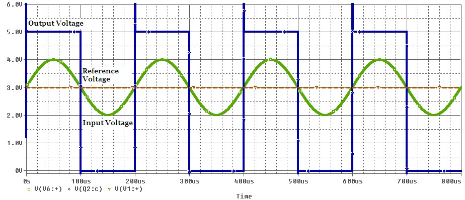
The circuit has a static reference voltage of 3V placed on the inverting (-) pin of the op-amp and a secondary input voltage on the non-inverting (+) pin for comparison. The figure below demonstrates how the comparator reacts to increasing input voltage. As you can see, once the green (input) voltage exceeds the red (reference voltage) the op-amp switches on the transistor and the voltage across the output goes from 0V to 5v. Some may have noticed that the rise from 0V to 5V is not instantaneous. The output starts to increase from zero around 2.8V on the input and does not reach the full 5V output until an input of about 3.2V. I do not want to get into the details in this blog entry, but I will address this slow rise in future blogs related to op-amps. Suffice it say for now the response time of the op-amp prevents ideal operation of the system as a whole.

The op-amp is operating in an “open loop” state in this design meaning that there is no feedback network from its output pin to its input pins. Op-amps are manufactured with very high open loop gains for reasons I will go into in future blogs. The high gain amplifies the difference in signal level between the op-amp inputs and drives the output to the rails (or equal to the voltage powering the op-amp). In this case, the rail voltage is 5V.

Figure 2. Input to Output Voltage Relationship of a Comparator 

Hopefully by now the basic operation of a comparator has been explored. The last figure shows what happens when a time-varying signal is introduced as an input and compared to the static input voltage.

Figure 3. Comparator Operation with a Time-Varying Input Signal

As you can see, each time the green input voltage drops below the red reference voltage the output of the system is driven low (0V). When green goes higher than red, the output is driven high (5V). The high frequency spikes at the beginning of the square wave output are a product of the switching components in the circuit diagram and are, again, something I will explore in future blogs. With a more robust design, you can get a more complete waveform using RC snubbers on the output.

Today, comparators can be found in thousands of ICs on the market either as stand-alone parts or integrated into more generalized chips. Control and logic schemes associated with these devices are much, much more complex than what I have discussed in this blog, but my goal is to give my readers at least a marginal understanding of the electronics that appear in nearly everything these days.

Feb 2, 2011

Tablets and Tech Convergence

Two years ago, a tablet computer was basically a laptop with optical character recognition (OCR). Since Apple launched the iPad in the Spring of 2010, “tablet” has taken on an entirely new association and created a new market. Some have gone as far to say that the iPad is a “breakthrough” device when it is really a product of technological convergence.
Technological convergence is the idea that niche devices will ultimately be incorporated into an all-in-one media solution. Before the release of tablets like the iPad or the Samsung Galaxy Tab, e-readers like the Amazon Kindle or the Barnes & Noble Nook were the dominant forms of personal media devices outside MP3 players and smart phones. Now, e-readers are taking a substantial hit from tablet growth and failing to meet projected sales numbers. While the e-reader is unlikely to be phased out completely, tablets have hindered their expansion by offering people a merger of an e-reader and a smartphone (minus the phone for now) in a package that amounts to a portable LCD screen. At this year’s CES there were over 100 new tablets on display, most of which were hidden behind walls of glass beyond the reach of salivating consumers. Complaints about the iPad go so far as to say it isn’t convergent enough with a lack of voice-over-internet protocol (VOIP) capability or a camera, but I attribute those deficiencies to Apple’s marketing department. The iPad 2 is slated for release in 2011 and all reports indicate it will be the iPad plus a camera.

The Apple 'iPad,' a new tablet computing device, is shown in this publicity photo from Apple released to Reuters on Wednesday.
The "revolutionary" iPad from Apple

While I do think that tablets have the ability to change the way we use technology, I also think their potential for backsliding is greater than any other portable media device available today. What happens when someone releases a tablet with a slide-out keyboard? Do we call it a giant smart phone or a netbook? Will netbooks even exist in 5 years as Moore’s law continues to improve computing power in smaller packages?
In the perpetual quest for a technological singularity, tablets will likely get closer than any consumer product in recent years. I have seen them dim lights, change channels, and control entire planetariums, but don’t toss out your remote just yet. The days of being able to dock your tablet in a desktop cradle for home use and carry it on the road during your daily commute are far away if they ever come. The rise of cloud computing makes this scenario somewhat practical yet still pretty unlikely.
I have no doubt that as tablets continue to evolve the lines between consumer products will become increasingly b lured. One day, people will look back and wonder why they paid money for superfluous gadgets when their tablet does it all; maybe there’s an app for that…


Jan 30, 2011

printf("Hello World! \n")

I am starting this blog so that my friend will stop telling me to start one. Hopefully this will mostly be an outlet for project ideas and tech news. I will also give some thoughts on research papers I come across every now and then.